List and briefly define the PCIe protocol layers.
PCI 익스프레스(PCI Express)는 2002년 PCI SIG가 책정한 입출력을 위한 직렬 구조의 인터페이스이며 인텔 주도하에 만들어졌다. 공식적인 약어로 PCIe로 표기한다. 옛 PCI, PCI-X와 AGP 버스를 대체하기 위하여 개발 되었다. PCIe는 앞서 언급한 버스 표준들과 비교하여 높은 시스템 버스 대역폭, 적은 I/O 핀 수, 적은 물리적 면적, 버스 장치들에게 더 뛰어난 성능 확장성, 상세한 오류 검출 및 보고 구조(Advanced Error Reporting (AER)[1]), 네이티브 핫-플러그 기능등 여러 장점을 가지고 있다. 최근에는 하드웨어 I/O 가상화도 지원한다.
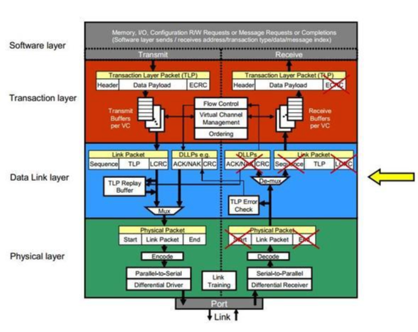
- Physical layer : Consists of the actual wires carrying signals as wel as circuitry and logic to support ancillary features required in the transmission and receipt of 1s and 0s.
- Data link : Is Responsible for reliable transmission and flow control. Data packets generated and comsumed by the DLL are called Data Link Layer Packets (DLLPs).
- Transaction : Generates and comsumes data packets used to implement load/store data transfer mechanisms and also manages the flow control of those packets between the two components on a link. Data packets generated and consumed by the TL are called Transaction Layer Packets(TLPs).
The hypothetical machine of Figure 3.4 also has two I/O instructions:
0011 = Load AC from I/O
0111 = Store AC to I/O
In these cases, the 12-bit address identifies a particular I/O device.
Show the program execution (using the format of Figure3.5) for the following program:
1. Load AC from device 5
2. Add contents of memory location 940.
3. Store AC to device 6.
Assume that the next value retrieved from device 5 is 3 and that location 940 contains a value of 2

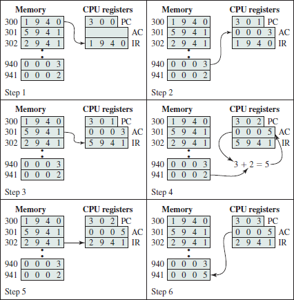
Step 1) (Load fetch) 3005 -> IR
Step 2) PC++
Step 3) (Load execute) 0003 -> AC
Step 4) (Add fetch) 5940 -> IR
Step 5) PC++
Step 6) (Add execute) 0003+0002=0005 -> AC
Step 7) (Store fetch) 7006 -> IR
Step 8) PC++
Step 9) (Store execute) 0005 AC -> Device 6
Consider a hypothetical microprocessor generating a 16 bit address (for example, assume that the program counter and the address registers are 16 bits wide) and having a 16-bit data bus.
| a. What is the maximum memory address space that the processor can access directly if it is connected to a "16-bit memory"? b. What is the maximum memory address space that the processor can access directly if it is connected to an "8-bit memory"? c. What architectural features will allow this microprocessor to access a separate "I/O space"? d. If an input and an output instruction can specify an 8-bit I/O port number, how many 8-bit I/O ports can microprocessor support? How many 16-bit I/O ports?. Explain |
a ) address length is 2^16 = 65536 bit. So approximately 64 kiloBytes is maximum memory address that processor can access direclty
b ) even though it is 8-bit memory, address length is 2^16. So approximately 64 kiloBytes is maximum memory address that processor can access direclty
c )
- need seperated I/O commands
- seperate command generate input signal when execution and create extra different output signals.
- created I/O signals is different to memory signal to it need one or more output pins to show the signals category
d ) if input and output instruction can specifyed by 8-biy I/O port number, 8-bit I/O port and 16-bit I/O support 2^8=256 because 00000000 ~ 11111111 (0~255) supportable port number is depend on microprocessor support ability.
A microprocessor has an increment memory direct instruction, which adds 1 to the value in memory location. The instruction has five stages: fetch opcode (four bus clock cycles), fetch operand address (three cycles), fetch operand (three cycles), add 1 to operand (three cycles), and store operand (three cycles).
|
a. By what amount (in percent) will the duration of the instruction increase if we have to insert two bus wait states in each memory read and memory write operation? b. Repeat assuming that the increment operation takes 13 cycles instead of 3 cycles. |
1 ) fetch opcode (4 cycles)
2 ) fetch operand address (3 cycles)
3 ) fech operand (3 cycles)
4) add 1 to operand (3 cycles)
5) store operand(3 cycles)
a ) without any insertion : 16 cylces(4+3+3+3+3)
when two bus wait states are inserted, each stages need two more clock cycles so in total 24 cycles (6+5+5+5+5).
Increased duration = Total wait state / Number of cycles without wait state
Total Wait State = 24 cylces - 16 cycles = 8 Clock cycles
Number of Cycles without wait state = 16 Clock cycles
So the answer is 8/16*100% = 50%
'Computer Science > Computer Architecture & Organization' 카테고리의 다른 글
| CA & CO Chapter 5 practice problem (0) | 2020.04.26 |
|---|---|
| CA & CO Chapter 4 practice problem (5) | 2020.04.21 |
| CA & CO Chapter 3 최상위에서 본 컴퓨터의 기능 및 상호 연결 (0) | 2020.04.15 |
| CA & CO Chapter 1 기본 개념과 컴퓨터 발전과정 (3) | 2020.04.15 |
| ISA 어셈블리 코드 해석하기 (0) | 2020.03.26 |


댓글